Report an Error


ATI Xbox 360 E GPU
- Graphics Processor
- Xenos Corona
- Cores
- 240
- TMUs
- 16
- ROPs
- 8
- Memory Size
- 512 MB
- Memory Type
- GDDR3
- Bus Width
- 128 bit

GPU

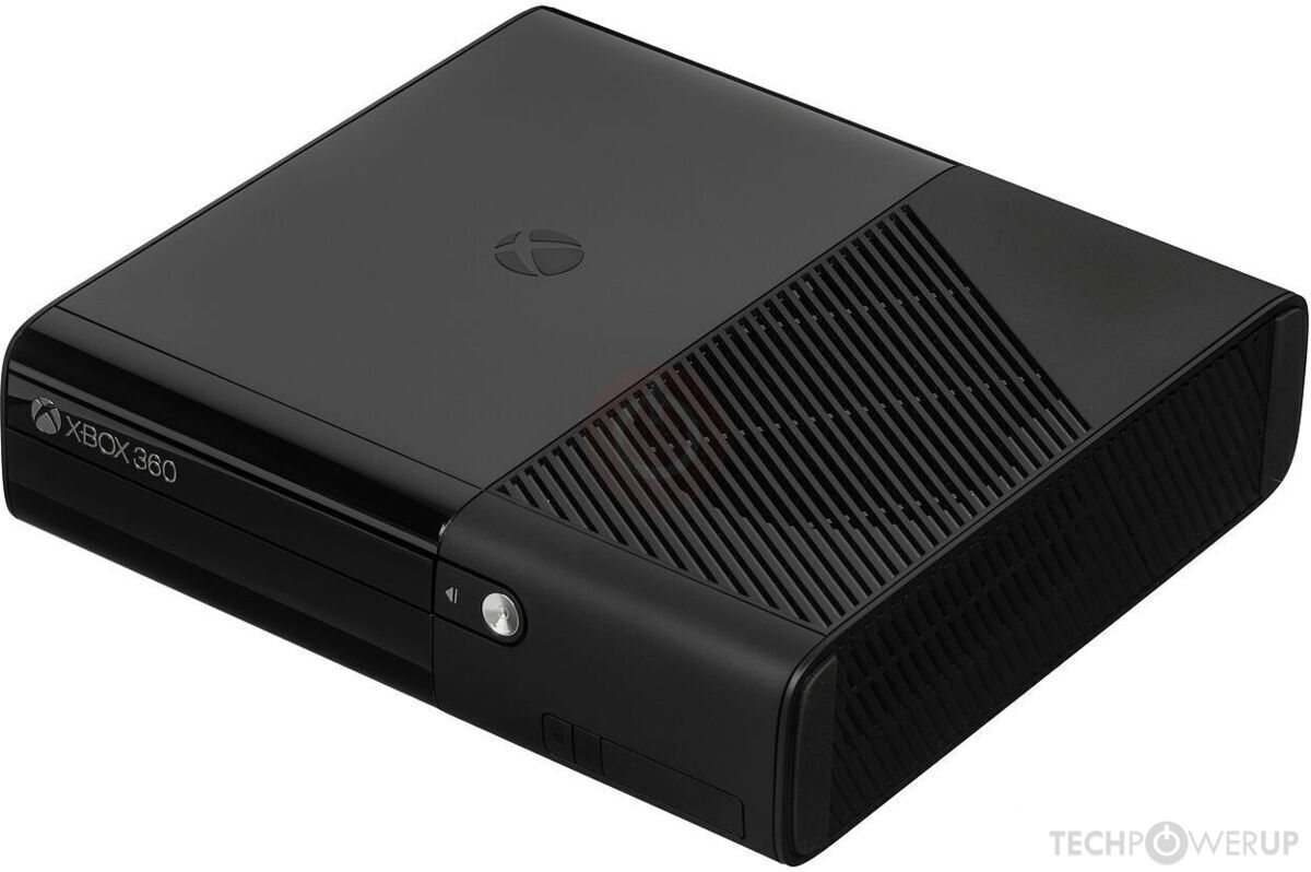
Front 2

Back
Recommended Gaming Resolutions:
- 640x480
- 1280x720
- 1366x768
The Xbox 360 E GPU was a performance-segment gaming console graphics solution by ATI, launched on June 10th, 2013. Built on the 45 nm process, and based on the Xenos Corona graphics processor, in its Crayola 6 variant, the device supports DirectX 9.0c. The Xenos Corona graphics processor is an average sized chip with a die area of 168 mm² and 372 million transistors. It features 240 shading units, 16 texture mapping units, and 8 ROPs. ATI includes 512 MB GDDR3 memory, which are connected using a 128-bit memory interface. The GPU is operating at a frequency of 500 MHz, memory is running at 700 MHz.
Its power draw is rated at 120 W maximum. The console's dimensions are 264 mm x 254 mm x 67 mm, and it features a igp cooling solution. Its price at launch was 299 US Dollars.
Its power draw is rated at 120 W maximum. The console's dimensions are 264 mm x 254 mm x 67 mm, and it features a igp cooling solution. Its price at launch was 299 US Dollars.
Graphics Processor
- GPU Name
- Xenos Corona
- GPU Variant
- Crayola 6
- Architecture
- TeraScale
- Foundry
- TSMC
- Process Size
- 45 nm
- Transistors
- 372 million
- Density
- 2.2M / mm²
- Die Size
- 168 mm²
Graphics Card
- Release Date
- Jun 10th, 2013
- Generation
-
Console GPU
(Microsoft)
- Production
- End-of-life
- Launch Price
- 299 USD
Clock Speeds
- GPU Clock
- 500 MHz
- Memory Clock
-
700 MHz
1400 Mbps effective
Memory
- Memory Size
- 512 MB
- Memory Type
- GDDR3
- Memory Bus
- 128 bit
- Bandwidth
- 22.40 GB/s
Render Config
- Shading Units
- 240
- TMUs
- 16
- ROPs
- 8
- Compute Units
- 3
Theoretical Performance
- Pixel Rate
- 4.000 GPixel/s
- Texture Rate
- 8.000 GTexel/s
- FP32 (float)
- 240.0 GFLOPS
Board Design
- Length
- 264 mm
10.4 inches
- Width
- 254 mm
10 inches
- Height
- 67 mm
2.6 inches
- Weight
- 2.9 kg (6.3 lbs)
- TDP
- 120 W
- Outputs
- 1x HDMI 1.2
Graphics Features
- DirectX
- 9.0c (9_3)
- OpenGL
- N/A
- OpenCL
- N/A
- Vulkan
- N/A
- Shader Model
- 3.0
Xenos Corona GPU Notes
| Transisters: CPU 140 million / GPU 232 million 48 floating-point vector processors for shader execution, divided in three dynamically scheduled SIMD groups of 16 processors each. Unified shading architecture (each pipeline is capable of running either pixel or vertex shaders) 10 FP ops per vector processor per cycle (5 fused multiply-add) Peak vertex count: 6.0 GVertices/s ((48 shader vector processors × 2 ops per cycle × 500 MHz) / 8 vector ops per vertex) for simple transformed and lit polygons Peak polygon count: 500 million triangles per second Peak shader operations: 96.0 billion shader operations/s (3 shader pipelines × 16 processors × 4 ALUs × 500 MHz) Floating Point Operations: 240.0 GFLOPS (3 shader pipelines × 16 processors × 500 MHz) MEMEXPORT shader function 16 texture filtering units 16 texture addressing units 16 filtered samples per clock Peak texel fillrate: 8.0 GTexel/s (16 textures × 500 MHz) 16 unfiltered texture samples per clock (16 texture addressing units) 8 Render Output units / pixel rendering pipelines Peak pixel fillrate: 4.0 GPixel/s without MSAA (8 ROPs × 500 MHz) Peak Z sample rate: 8.0 GSamples/s (2 Z samples × 8 ROPs × 500 MHz) 32.0 GSamples/s using 4X anti aliasing (2 Z samples × 8 ROPs × 4X AA × 500 MHz) Peak anti-aliasing sample rate: 16.0 GSamples/s (4 AA samples × 8 ROPs × 500 MHz) Peak Dot product operations: 24 billion per second Support for a superset of DirectX Xbox 360 10 MiB daughter embedded DRAM (at 256GB/s) framebuffer on NEC designed eDRAM die includes additional logic 105 million transistors (192 parallel pixel processors) for color, alpha compositing, Z/stencil buffering, and anti-aliasing called “Intelligent Memory”, giving developers 4-sample anti-aliasing at very little performance cost. |
May 3rd, 2024 16:49 EDT
change timezone
Latest GPU Drivers
New Forum Posts
- AM5 Motherboard Question, which of these two should I go with? (8)
- My Laptop is having issues with PL2 and EDP OTHER (7)
- 2019 LTSC vs 2021 LTSC (5)
- Announcement: VPN's no longer work right in Windows 10 or 11 or Servers (26)
- new Gigabyte B450 mobo won't post (1)
- Old high quality PSU, or semi-old mid-quality PSU? (59)
- Optane 1600X 118GB - Lots of CDM benching and some thoughts (64)
- Ryzen 7800x3d $196 with bundle at Microcenter (19)
- Looking for recommendations to upgrade the GPU (42)
- FINAL FANTASY XIV: Dawntrail Official Benchmark (79)
Popular Reviews
- HYTE THICC Q60 240 mm AIO Review
- ASRock NUC BOX-155H (Intel Core Ultra 7 155H) Review
- Meze Audio LIRIC 2nd Generation Closed-Back Headphones Review
- Montech Sky Two GX Review
- Ugreen NASync DXP4800 Plus Review
- Upcoming Hardware Launches 2023 (Updated Feb 2024)
- Team Group T-Force Vulcan ECO DDR5-6000 32 GB CL38 Review
- MOONDROP x Crinacle DUSK In-Ear Monitors Review - The Last 5%
- Finalmouse UltralightX Review
- AMD Ryzen 7 7800X3D Review - The Best Gaming CPU
Controversial News Posts
- Intel Statement on Stability Issues: "Motherboard Makers to Blame" (235)
- Windows 11 Now Officially Adware as Microsoft Embeds Ads in the Start Menu (167)
- Sony PlayStation 5 Pro Specifications Confirmed, Console Arrives Before Holidays (117)
- AMD's RDNA 4 GPUs Could Stick with 18 Gbps GDDR6 Memory (114)
- AMD to Redesign Ray Tracing Hardware on RDNA 4 (111)
- NVIDIA Points Intel Raptor Lake CPU Users to Get Help from Intel Amid System Instability Issues (106)
- AMD "Strix Halo" Zen 5 Mobile Processor Pictured: Chiplet-based, Uses 256-bit LPDDR5X (103)
- AMD Ryzen 9 7900X3D Now at a Mouth-watering $329 (103)