What Is a Solder Mask Used For?
Rayming PCB & Assembly
Printed Circuit Board Manufacturing and PCB Assembly Services
A solder mask, also known as solder resist, is a thin lacquer-like layer of polymer that is usually applied to the surface of a printed circuit board (PCB) as one of the final finishing steps in the PCB fabrication process. The solder mask serves several important functions for the PCB:
Protecting the Copper Traces
One of the main purposes of the solder mask is to protect the delicate copper traces on the PCB from environmental damage and corrosion. The thin copper traces that connect the various components on a PCB can easily be scratched or contaminated during handling and assembly. The solder mask covers over and seals the copper traces, shielding them from physical and chemical damage.
Preventing Solder Bridges
Another vital function of the solder mask is preventing solder bridges from forming between closely spaced PCB traces during soldering. Solder mask acts as a solder dam - when solder paste is applied on masked areas during assembly, the solder builds up to the edge of the mask but does not bridge across to adjacent traces. This allows much higher circuit densities without short circuits.
Providing Insulation
The solder mask layer is typically made from an electrically insulating polymer material. This provides extra insulation between closely spaced copper traces on high density boards. It also prevents traces on the board from shorting if they come into contact with external metal components or the enclosure chassis.
Marking Solder Areas

Openings are formed in the solder mask wherever a solder joint needs to be made to a component lead or a surface mount pad. This clearly marks the intended solder locations. During reflow soldering, the solder paste only adheres to these openings, avoiding solder build up on other areas of the board.
Protecting Board Against Contamination
The solder mask seals the entire surface of the PCB, protecting against contamination and oxidation during assembly and use. This helps prevent dendritic growth and other reliability issues caused by surface contamination.
Improving Aesthetics
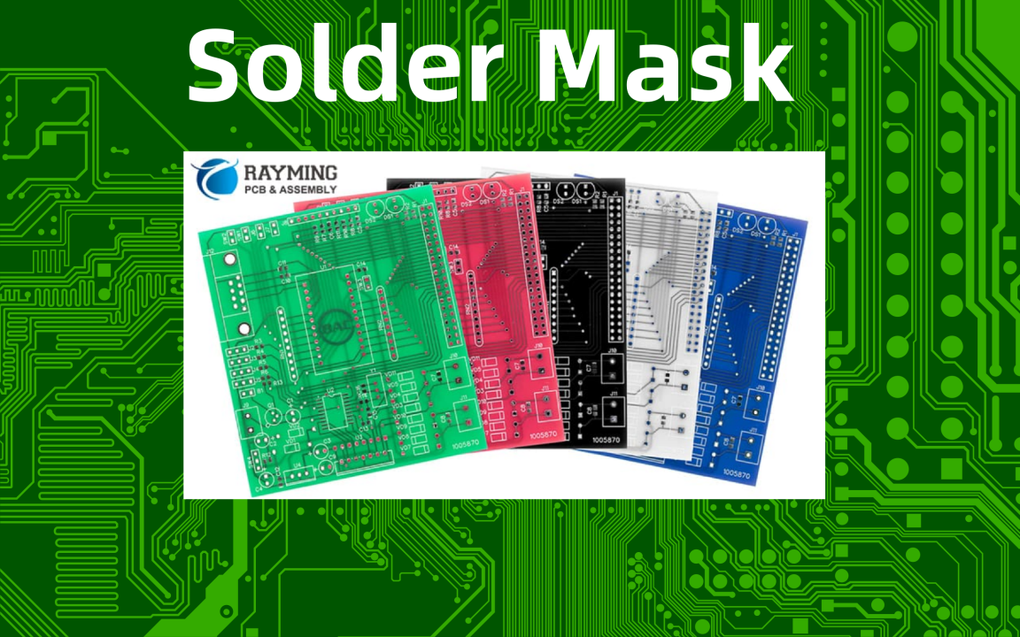
Solder mask is typically applied in a single uniform color like green, blue, red or black. This gives assembles boards a more consistent and professional look. The label printing and markings can stand out clearly against the mask background.
Types of Solder Masks
There are two primary types of solder mask used in PCB fabrication and assembly:
Liquid Photoimageable Solder Masks (LPISM)
LPISM is the most common solder mask type used today. It is a two part system consisting of a liquid polymer mixed with a light sensitive catalyst. The LPISM layer is applied by screen printing, curtain coating or spray coating on the PCB surface. It is then exposed to UV light through a mask template and developed like a photographic film to form openings. The final curing is done at high temperatures.
Dry Film Solder Masks
As the name suggests, dry film solder masks come pre-formed on a polymer carrier film. The film is laminated onto the PCB and then imaged using photolithography process. After developing and curing it forms the required protective coating. Dry film masks provide tighter dimensional control but liquid masks can coat more complex board geometries.
Solder Mask Properties
Solder mask materials are formulated to have properties optimized for the PCB protection role:
- Chemical resistance - high resistance to solvents, fluxes and other chemicals used in PCB fabrication to prevent smearing or swelling.
- Temperature resistance - Ability to withstand soldering process temperatures up to 260°C without charring, cracking or losing adhesion.
- Flexibility - Mask should be flexible enough to withstand some board flexing without cracking.
- Adhesion - Excellent adhesion to the PCB substrate over the entire surface to prevent peeling or separation.
- Resolution - Ability to produce fine openings and resist patterns to at least 150 microns.
- Photo-definition - Good imaging characteristics and clean development of exposed areas.
- Solder resistance - Prevent wicking of solder into masked areas during reflow while allowing solder build up only in open areas.
Application of Solder Mask
The solder mask is typically applied at the end of the PCB fabrication process as one of the final finishing steps, after all etching and plating is completed. The application process consists of the following sequence:
- Surface Preparation - The copper traces are cleaned to remove any oxidation or contamination. A chemical microetch is performed to roughen the copper surface and improve mask adhesion.
- Mask Application - Liquid masks are applied by curtain coating, screen printing or spray coating. Dry film masks are laminated using heat and pressure. The mask layer is applied over the entire board surface.
- Imaging - A photographic mask is used to transfer the pattern of openings onto the mask layer. Liquid masks are imaged using UV light while dry masks use visible or UV light.
- Developing - The board is developed in a chemical solution to remove the unexposed areas of the mask, leaving behind the required openings.
- Curing - A thermal cure "hardens" the mask material, improving chemical and heat resistance. Typical curing is done at 150-200°C.
- Excess Mask Removal - Any residual solder mask in the openings is gently ablated away using plasma etch techniques. This ensures good solderability.
- Final Finish - A layer of organic protective coating is sometimes applied over the cured solder mask surface for additional protection.
Solder Mask Defects

Some typical solder mask defects, their causes and solutions are listed below:
DefectDescriptionCauseSolutionInsufficient OpeningOpenings in mask are undersizedUnderexposure during imagingIncrease exposure energySolder Mask SmearMask material inadvertently deposited in openingsMask surface not adequately cured prior to developingEnsure proper mask cure before developmentPinholesMicroscopic pores in the mask surfaceContamination preventing mask adhesionImprove surface cleanliness prior to coatingBlisteringSmall air bubble pockets under the maskMoisture contamination; poor adhesionImprove surface preparation and dryingDelaminationLarge area peeling of maskPoor adhesion; thermal stressUse adhesion promoter; improve lamination processBridgingSolder mask residue bridging adjacent padsInadequate developingIncrease developing time and agitationDark or Burned SpotsDiscolored burnt areas on maskShadow areas during exposure; heating issuesDiffuse UV light; check thermal process
Solder Mask Design Guidelines
To achieve good solder mask results consistently, designers should follow these guidelines:
- Provide a sufficient mask web of ≥150μm between adjacent conductors
- Mask defined openings should be ≥200μm larger than pad size
- Minimum mask web width should be ≥100μm
- Avoid acute angles with mask. Use rounded pad shapes.
- Follow recommended solder mask and conductor overlap margins
- Allow slightly larger openings for plated through hole pads
- Verify all openings are clearly defined on the solder mask layer
Following these guidelines prevents common defects like bridging and insufficient openings.
Solder Mask Repair
Minor solder mask defects can sometimes be repaired after fabrication:
- Insufficient openings can be enlarged by additional light imaging and developing.
- Smears may be removed by plasma etching in small localized areas.
- Bridging can be ablated away using a laser micromachining system.
But any extensive repairs require the complete mask to be stripped and reapplied, which is not always feasible if components are already mounted.
Importance of Solder Mask

In summary, a properly applied high quality solder mask is critical for:
- Protecting PCB copper traces from environmental and physical damage
- Preventing solder bridges that can cause short circuits
- Providing insulation between conductors
- Accurately defining solder locations
- Shielding the board surface from contamination
- Giving assembles boards a professional finished appearance
Solder mask is what transforms a bare PCB into a robust printed circuit assembly, capable of withstanding assembly processes, thermal cycling and long term use. The trend towards higher density boards and assemblies makes high performance solder mask more crucial than ever.
Frequently Asked Questions
What are the different types of solder mask?
The two main types of solder mask are liquid photo-imageable (LPISM) and dry film solder mask. LPISM is more widely used while dry film offers tighter resolution.
Does solder mask go on before or after soldering components?
Solder mask is applied during PCB fabrication, before any components are soldered onto the board. It becomes the background layer that components solder onto.
Can you apply solder mask yourself?
Manual solder mask application is challenging. It's best applied using industrial processes like screen printing by the PCB manufacturer. Attempting to coat it yourself risks many defects.
Is solder mask required for every PCB?
While not absolutely mandatory, applying solder mask is considered essential for most PCB types to protect against environmental damage and prevent shorts. Bare PCBs have limited functionality.
Can you solder through solder mask?
Solder mask is designed to be selectively opening in required areas to allow soldering to the exposed pads. Solder will not wet to the mask itself, avoiding bridging issues.