At last time, we shared a blog talking about Why most of the PCB boards are green?. Believe you’ve known the reasons for why most of solder mask colors are green.
Today, let’s share something about the function of solder mask on the Printed Circuits Boards.
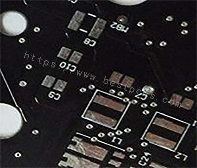
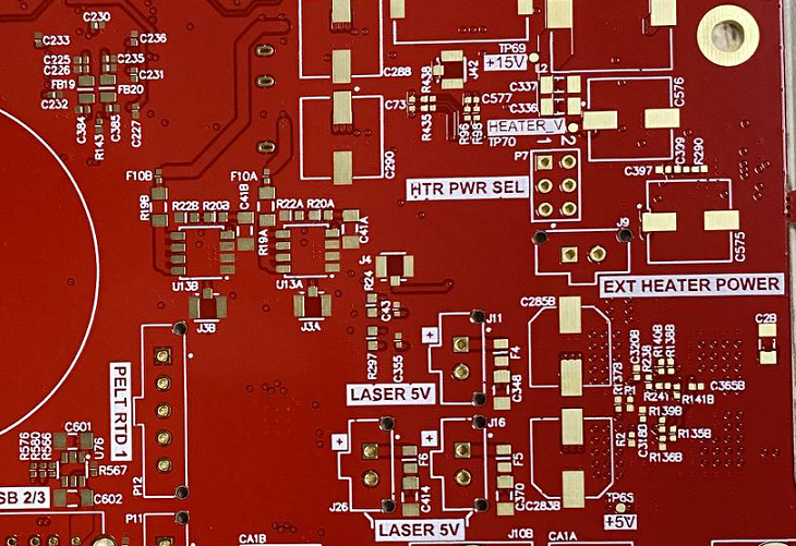
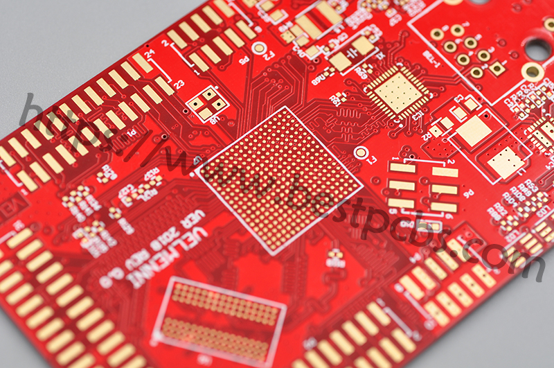
The solder mask layer is designed mainly to prevent the PCB copper foil from being directly exposed to the air and play a role in protecting the PCB surface, which is also to prevent the area that should not be soldered from being soldered.
As we know that almost all the PCB need to do the assembly, which need to go through the reflow soldering while the assembly, and solder mask plays an important role during control of the reflow soldering process.
Here is a summary for what solder mask roles played on the board:
(1) Prevent physical disconnection of conductor circuits on the circuits board;
(2) In the welding process, solder mask can prevent short circuit caused by bridging;
(3) solder mask can reduce copper pollution to the soldering trough;
(4) Print solder mask on the PCB can prevent insulation deterioration and corrosion caused by external environmental factors such as dust and moisture;
(5) Solder mask are with high insulation; it is possible to increase the density of the circuit.
In terms of solder mask material, it must be used through liquid wet process or dry film lamination.
Dry film solder mask materials are supplied in a thickness of 0.07-0.1mm (0.03-0.04″), which can be suitable for some surface mount products, but this material is not suitable for PCBs with tighter pitches.