 One of the downsides of home-made CNC printed circuit boards is that a lot of the copper cladding remains and can lead to short circuits when solder strays onto the common waste area outside the formed tracks. Also, after a while it tarnishes and does not look great.
One solution to both these problems is to apply a solder mask over everything that is not meant to have solder on it, similar to professionally made boards.
Solder mask paint is available for sale online in a selection of colors. It is basically a water-repelling type of paint that needs to be cured under UV light. There are also many sources for how to do a DIY solder mask (such as this Instructable or this YouTube video), so I decided to ‘try this at home’.
The two main ingredients to do this are Solder Mask Paint (ordered from one of many shops on eBay) and a lamp for the UV Curing, as I did not want to just rely on sunshine.
Making the UV Curing Lamp
UV curing is common in many nail (as in in fingernail) salons. These have ‘oven’ like cavities into which the fingernails are placed to cure the paint under light generated by UV LEDs. Some research online showed that these looked like they would be simple build at a fraction of the cost of a bought one, especially as I already had 50 UV LEDs on hand.
As with all diffuse light sources, the intensity of the light decreases rapidly with the distance from the source. So placing the LED too far from the paint increases the curing time. Another important consideration is to ensure a uniform light coverage on the surface of the paint – this comes down to the distance between the LED light sources. Too close and there will be gaps in the light coverage between LEDs; too far and there is overlap with more light intensity in the overlap areas.
 Some basic geometry provided the relationship between the height of the LED from the surface of the PCB (h) and the spread of the cone of light from the LED (d) that would be ‘just right’ that would ensure maximum coverage for the LEDs and a uniform light intensity.
The datasheets for my LEDs quoted a light cone spreading 120° from the point source, making the half the angle (α) 60°.
I was planning to use a 3″ x 4″ prototyping board for mounting the LEDs, so the distance between LEDs was going to be a multiple of 0.1″ (2.54mm) – the hole spacing on the protoboard.
Using the formula, h was calculated for a whole number multiples of spacing for d. I decided to settle on a spacing 5 holes apart (12.7mm or ½”), shown below, which resulted in a height h of about 3.6mm, which seemed close but reasonable given the wide angle for the LEDs used. Coincidentally, this arrangement on the protoboard needed 48 LEDs, which also suited the quantity on hand.


The next calculation was to work out the power requirements for the light panel. I measured the individual LED voltage drop as 3.2V, and the light intensity seemed to reach a good level at around 20mA. To minimize the number of resistors, I put 3 LEDs in series. With a 12 V power supply, a 100Ω resistor drops the remaining 2.2V and limits the current to 20mA. For 48 LEDs, the power supply needs to power 16 groups in parallel, or 320mA total. A suitable wall wart was obtained!
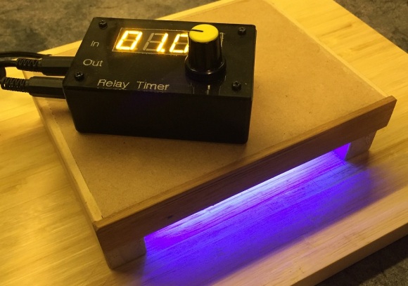
Scrap wood and MDF were cobbled together to contain the lamp, paying attention to keep the height to the calculated value. The lamp ‘panel’ was then screwed to the underside of the box lid. The Relay Timer described in a previous post is used to control the power on/off and time the UV exposure.
Solder Masking a PCB
To produce the solder mask, I followed the basic flow described in this video (which I won’t repeat here). Eagle CAD can be used to print the pad masks by turning off all the drawing layers except pads and vias. I printed mine on a laser printer and they worked fine.
The results weren’t too bad for a first attempt (photos below) and I am sure my technique will develop. The process was pretty fast – around 20 minutes from cleaning the board to having a completed (if flawed) product that adequately protected the PCB during the subsequent assembly and soldering process.


Things that I learned to do better next time:
- Wear gloves! This stuff is sticky and it gets everywhere. Make sure that work areas are adequately protected as well, both when spreading and while cleaning off.
- I need to experiment with exposure times. This first attempt over-cured the paint, making it necessary to use a hard scraper to remove what was supposed to be uncured paint from the solder pads. Trying to clean off the pads removed the paint in areas that later need to be touched-up. Worth trying to use cotton buds soaked in thinner to clean the pads rather than a general wiping action.
- Through holes in the PCB are a problem, as they fill with paint and then need to be individually cleaned out at the end of the process. Drilling the holes after masking is an option but negates the accuracy of doing this on the CNC.
Update 21 Aug 2016
One cause for over curing into the pads are the very small pads that Eagle CAD has by default for many components. I am guessing that the UV light bleeds through the plastic sheet. Creating parts with larger oval solder pads has fixed this problem.
I also started to dilute the solder mask paint with a few drops of rubbing alcohol before spreading it out. This makes the paint less viscous and it is easier to spread.
To avoid clogging through holes but still get the CNC positioning accuracy, I spot drill the holes when making the board and then fully drill them out when the PCB is completed. This adds step to the process but takes less time than unclogging the pre-drilled holes.

5 replies on “UV Curing Lamp for DIY PCB Solder Mask”
OK now I get it. Thanks for your answers!
LikeLike
Hi Marco, I wanna ask you something. My UV LEDs come with no datasheet, but the seller tells that its light viewing angle is about 20°~25°. Why is there too much difference range between my LEDs and your LEDs.
Please reply as soon as you can.
Thanks!
LikeLike
The top of the LED acts like a lens and manufacturers can engineer this to produce a narrow or wider beam or a to suit different applications. This is very common in IR LEDs and it seems also happens in UV LEDs.
LikeLike
Hi, thanks for your answer anyway. But one thing still stucked in my mind is, how could you get 30mm as your calculated height of your LEDs from the bottom surface. I still didn’t get it.
I’ve tried using the above formula to calculate mine (and also calculate yours) but didn’t get the exact results as yours.
Thanks in advance.
LikeLike
I rechecked and you are right. The formula give about 3.6mm height for the LEDs, so there was a mistake in the text which is now fixed. The actual height of the LEDs inside the box was around 10mm as I also had to take into account the thickness of the PCB and the support I use to move it around. The LEDs are about 4-5mm above the surface of the PCB when this is taken into account, so it looks like it was made correctly, just written up wrong.
LikeLike